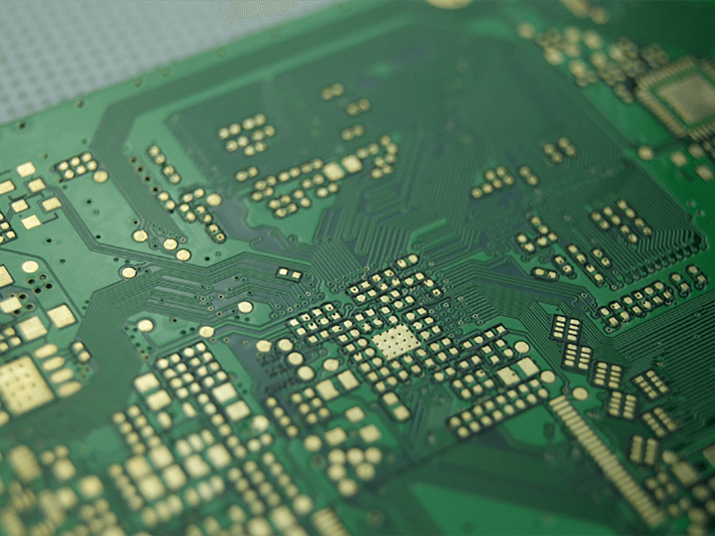
PCB Capabilities
Full Range of PCB Capabilities to Fit Your PCB Manufacturing Needs
In the field of high-end printed circuit board manufacturing, we always maintain efficient delivery capabilities, combined with the high quality of production management, research and development PCB manufacturing capabilities, manufacturing capabilities and construction of PCB core technologies, accelerating technological innovation and development.
Listed below are UETPCBA’s PCB manufacturing capabilities. We are focused on providing high-quality printed circuit boards to fit all of your needs.
Detailed Printed Circuit Board Assembly Capabilities
| Standard Features | Standard | Advanced |
|---|---|---|
| Maximum Layer Count | 20 | 48 |
| Maximum Panel Size | 533x610mm [21×24″] | 610x1067mm [24×42″] |
| Outer Layer Trace/Spacing | 90µm/90µm | 64µm/76µm |
| (1/3oz starting foil + platig) | [0.0035″/0.0035″] | [0.0025″/0.003″] |
| Inner Layer Trace/Spacing | 76µm/76µm | 50µm/50µm |
| (Hoz inner layer cu) | [0.003″/0.003″] | [0.002″/0.002″] |
| Maximum PCB Thickness | 3.2mm [0.125″] | 6.5mm [0.256″] |
| Minimum PCB Thickness | .20mm [0.008″] | .10mm [0.004″] |
| Minimum Mechancial Drill Size | .20mm [0.008″] | .10mm [0.004″] |
| Minimum Laser Drill Size | .10mm [0.004″] | .08mm [0.003″] |
| Maximum PCB Aspect Ratio | 10:1 | 25:1 |
| Maximum Copper Weight | 5 oz [178µm] | 6 oz [214µm] |
| Minimum Copper Weight | 1/3 oz [12µm] | 1/4 oz [9µm] |
| Minimum Core Thickness | 50µm [0.002″] | 38µm [0.0015″] |
| Minimum Dielectric Thickness | 64µm [0.0025″] | 38µm [0.0015″] |
| Minimum Pad Size Over Drill | 0.46mm [0.018″] | 0.4mm [0.016″] |
| Solder Mask Registration | ± 50µm [0.002″] | ± 38µm [0.0015″] |
| Minimum Solder Mask Dam | 76µm [0.003″] | 64µm [0.0025″] |
| Copper Feature to Edge, V‐cut (30°) | 0.40mm [0.016″] | 0.36mm [0.014″] |
| Copper Feature to PCB Edge, Routed | 0.25mm [0.010″] | 0.20mm [0.008″] |
| Tolerance on Overall | ± 100µm [0.004″] | ±50µm [0.002″] |
| Dimensions |
| HDI Features | Standard | Advanced |
|---|---|---|
| Minimum Microvia Hole Size | 100µm [0.004″] | 75µm [0.003″] |
| Capture Pad Size | 0.25mm [0.010″] | 0.20mm [0.008″] |
| Glass Reinforced Dielectrics | Y | Y |
| Maximum Aspect Ratio | 0.7:1 | 1:1 |
| Stacked Microvias | Y | Y |
| Copper Filled Microvias | Y | Y |
| Buried Filled Vias | Y | Y |
| Maximum No. of Buildup Layers | 3+N+3 | 5+N+5 |
PCB Materials
| FR4 Standard Tg | Shengyi, ITEQ, KB, Nanya |
|---|---|
| FR4 Mid Tg | Shengyi S1000, ITEQ IT158 |
| FR4 High Tg | Shengyi S1000‐2, S1170 |
| EMC EM827 | |
| Isola 370HR | |
| ITEQ IT180A | |
| Panasonic R1755V | |
| High Performance | EMC EM828, EM888(S), EM888(K) |
| Isola FR408, FR408HR | |
| Isola I‐Speed, I‐Tera MT | |
| Nelco N4000‐13EP, EPSI | |
| Panasonic R5775 Megtron 6 | |
| RF Materials | Rogers RO4350, RO3010 |
| Taconic RF‐30, RF‐35, TLC, TLX, TLY | |
| Taconic 601, 602, 603, 605 | |
| Halogen Free | EMC EM285, EM370(D) |
| Panasonic R1566 | |
| Aluminum Backed PCB | Shengyi SAR20, Yugu YGA |
Surface Finishes
| Electroless Nickel Immersion Gold (ENIG) |
| Hot Air Solder Level (HASL, Lead and Lead‐free) |
| OSP, Immersion Tin,Immersion Silver, ENEPIG |
| Gold Fingers, Flash Gold, Full Body Hard Gold, Wire Bondable Gold |
| Selective and Multiple Surface Finishes |
| Carbon Ink, Peelable SM |
This is heading text
High volume PCB Assembly refers to bulk printed circuit board assembly projects of 10,000 pieces or more, in one cycle of production with DFM and DFT. This is highly popular in high-end modern electronic manufacturing companies.
The benefits of high volume PCB Assembly are
- One-time design and prototyping services
- Faster time-to-market
- cost-efficient as you can purchase in bulk
- Consistent quality
- Production uniformity
- Shortened production cycles
Choosing a high volume PCB manufacturing company is quite a daunting task in this cut-throat competitive space. Two of the most common things one looks for in any company are quality and cost-effectiveness. Besides, you can also look into their experience, manufacturing capabilities, turnaround time, responsiveness, value for time & money, flexibility, and customization options.
Mer-Mar Electronics is a USA-based PCB fabrication and manufacturing company with over 4 decades of experience in PCB assembly services. We are an ISO-certified and ITAR-compliant company. We offer high volume circuit boards in the least turn-around time, flexible shipment plans, and at competitive prices. We follow a client-centric approach to ensure guaranteed quality satisfaction.
You can send your Gerber files and BOM to us We would provide you the quote Give your confirmation and the order We start with PCB fabrication component procurement We perform soldering and testing Finally, we go for packaging and shipping to you.
Well, we can accurately present the time based on the complexity of your board. Let us first go through your Bill of Materials (BOM) and Gerber files. See how much time it takes.
Yes, we do. After the PCB assembly, we can launch an x-ray test on your components. The additional charges will be levied after the assembly test.
We make sure you face zero issues. However, if unfortunately, you face any problems with the boards, please send high-resolution images for proper evaluation. If we get a confirmation of the root cause, we will take responsibility for your board repairs.
As part of the high volume production process, we provide components and parts procurement for optimizing the manufacturing process at zero price. Also, repeat customers may also take advantage of loyalty discounts to reduce the long-term costs of production. Depending on your requirements, we would let you know the final costs.
Yes. We do offer reliable customer support for your orders from start to finish. We will walk you through every step of the process and our PCB experts will also be available all the time.