


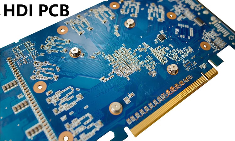
High-density interconnect (HDI) printed circuit boards (PCBs) are an indispensable part of modern electronic products. They are widely used in various electronic devices, such as smartphones, tablets, laptops, wearable devices, etc., with their superior performance and design flexibility. This article will explore the characteristics, advantages and applications of HDI PCB multilayer boards in the field of electronic products.
Characteristics of HDI PCB
HDI PCB is a high-density, high-performance circuit board technology, and its main features include:
Higher circuit density: By using thinner wires, smaller vias and denser device layout, HDI PCB can achieve more complex circuit design in a limited space.
Multilayer structure: HDI PCBs usually adopt a multilayer structure, which enables them to support complex circuit wiring and meet the needs of high-performance electronic products.
Miniaturized design: Due to the high-density characteristics of HDI PCBs, they are very suitable for use in miniaturized electronic products.
Advantages of HDI PCB
Improved performance: HDI PCB can significantly improve signal integrity and transmission speed to meet the requirements of high-speed data transmission.
Save space: Due to its high-density design, HDI PCBs are able to integrate more functions in a limited space, helping to design more compact devices.
Reduce weight: Compared with traditional PCBs, HDI PCBs can reduce material usage, thereby reducing product weight, making them ideal for portable electronic devices.
Improve reliability: The multi-layer design of HDI PCBs helps reduce signal interference and improve circuit reliability.
Applications of HDI PCBs
Smartphones and tablets
Smartphones and tablets are one of the most widely used areas for HDI PCBs. Since these devices have extremely high requirements for performance and size, the high density and multi-layer design of HDI PCBs can well meet these needs.
Wearable devices
HDI PCBs are also widely used in wearable devices. Since wearable devices need to be small and light, HDI PCBs can achieve complex functions in a small volume.
Automotive electronics
With the increasing degree of automotive electronics, HDI PCBs are increasingly used in this field. They are used in in-vehicle navigation systems, entertainment systems, and advanced driver assistance systems (ADAS), etc.
Medical Devices
In medical devices, HDI PCBs are used to manufacture high-precision miniaturized devices such as portable monitoring devices and implantable medical devices.
HDI PCB multilayer boards have become key components in the design of modern electronic products with their excellent performance and design flexibility. As electronic products develop towards higher performance and smaller size, the application of HDI PCBs will become more extensive. In the future, with the further development of technology, HDI PCBs will bring more innovations and possibilities to electronic products.