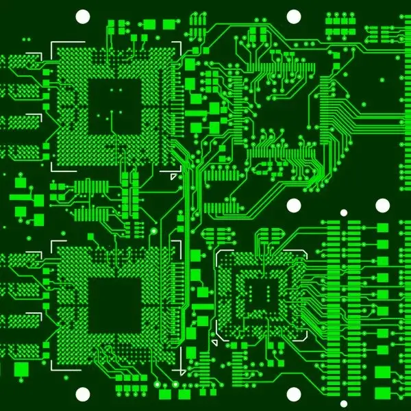
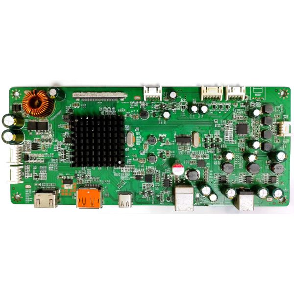
Printed circuit board design is based on the circuit diagram, circuit designers need to achieve the function.
Printed circuit board design is based on the circuit diagram, circuit designers need to achieve the function. Printed circuit board design mainly refers to layout design, need to consider the layout of external connection. Optimized layout of internal electronic components. Optimized layout of metal wire and through hole. Electromagnetic protection. Heat dissipation and other factors. Excellent layout design can save production cost and achieve good circuit performance and heat dissipation performance.
PCB Layout Matters Needing Attention
(1) Avoid arranging important signal lines on the edge of PCB, such as clock and reset signal.
(2) The interval between the ground wire and signal line of the chassis shall be at least 4mm;Keep the length-width ratio of the ground wire of the housing less than 5:1 to reduce the inductance effect.
(3) The device and wire in the determined position will be locked with the LOCK function, so that it will not be mistakenly moved in the future.
(4) The minimum width of wire should not be less than 0.2mm (8mil). In high-density and high-precision printed lines, the width and spacing of wire can generally be 12mil.
(5) The principle of 10-10 and 12-12 can be applied for wiring between IC pins in DIP package. That is, when two pins pass through two wires, the diameter of the pad can be set as 50mil, the width and spacing of the pad can be set as 10mil, and when only one wire passes between two legs, the diameter of the pad can be set as 64mil, and the width and spacing of the pad can be set as 12mil.
(6) When the diameter of the pad is 1.5mm, in order to increase the stripping strength of the pad, the length and width of the pad shall be no less than 1.5mm and the circular pad shall be adopted.
(7) When the wiring of the welding pad connection is relatively thin, the connection between the welding pad and the wiring should be designed as a water drop, so that the welding pad is not easy to peel and the wiring and the welding pad are not easy to disconnect.
(8) In the design of large-area copper application, there should be an open window on the copper application, heat dissipation holes should be added, and the open window should be designed into a network.
(9) Shorten the connection between high-frequency components as far as possible, and reduce their distribution parameters and mutual electromagnetic interference. Vulnerable components should not be too close to each other, input and output components should be as far away as possible.
Hot Tags: industrial remote control PCB layout, China, manufacturers, suppliers, factory, customized, made in China, LED Aluminum Printed Circuit Board, 2 Layer Heavy Copper Power PCB Board, Turnkey Medical Electronic Circuit Board Assembly, Aerospace System PCB Board, Smart Home Camera PCB Assembly, Wifi Router PCB Assembly


