
Our company specializes in providing customers with reliable products and good service.
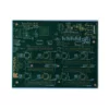
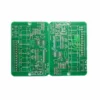
HDI is the abbreviation of high density interconnector. It is a kind of printed circuit board (PCB) production technology. It uses micro blind buried hole technology to produce PCB with high density. HDI is a compact product designed for small capacity users.
Product Advantages:
1.It can reduce the cost of PCB: when the density of PCB increases more than eight layers,
the cost of manufacturing with HDI will be lower than that of traditional complex pressing process.
2.Increase circuit density: interconnection between traditional circuit board and parts
3.Conducive to the use of advanced construction technology
4.Better electrical performance and signal correctness
5.Better reliability
6.Improved thermal properties
7.Improve RFI / EMI / ESD
8.Increase design efficiency
Company Advantage:
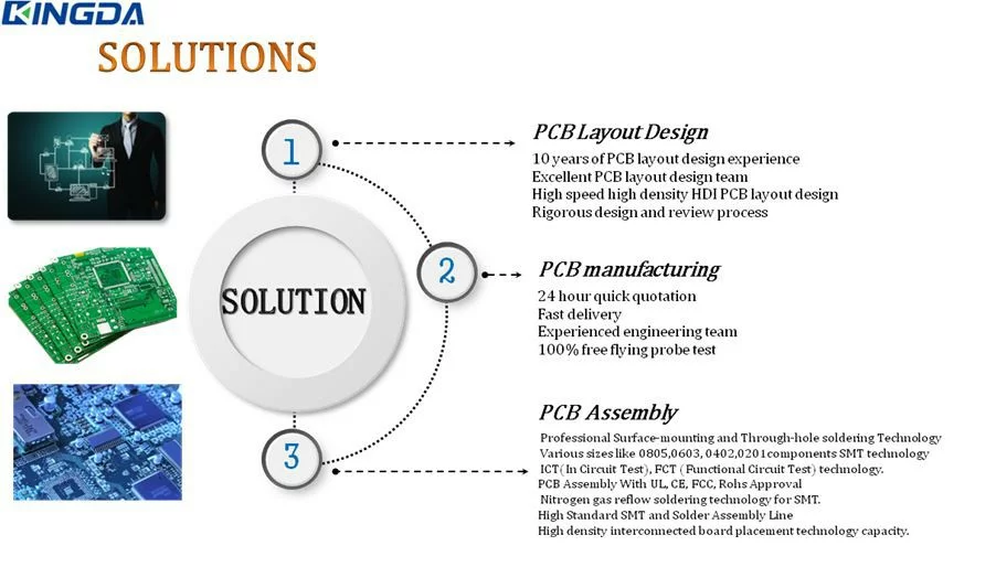
Our factory has over 10 years of experience in PCB production and assembly.
Market:
The main market is in Europe, South America, Southeast Asia, and Australia.
Hot Tags: multilayer hdi pcb, China, manufacturers, suppliers, factory, customized, made in China, FR4 Electronic Circuit Board Assembly, Smart Speaker PCB Assembly, Automation Control PCB Assembly, Rigid PCB, Control Printed Circuit Board, PCB Assembly For Medical Devices.