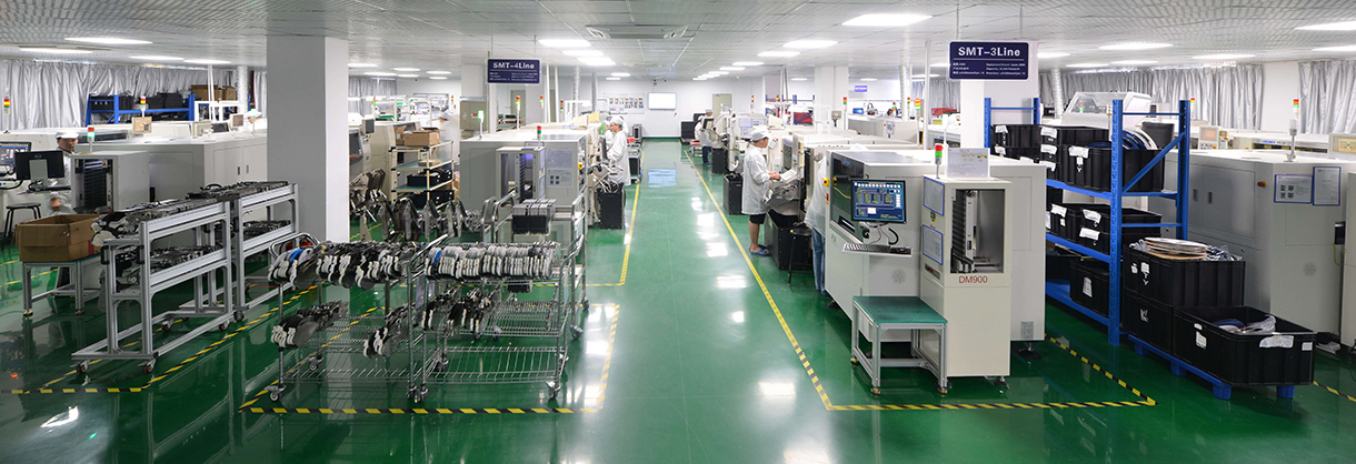
Quality Management
Quality Management

Pre-production Check:
Confirm PCB specifications: material, thickness, copper thickness, layers, stack-up, finish surface, solder mask and so on.
Correct designators of components and clear silkscreen with orientation
Complete component descriptions of manufacturer, P/N, designator and QTY in BOM
Correct pick & place file
SMT Process: with lead/lead-free
Complete procedure of programming and function test
Other special requirements
New Product Introduction:
Make clear customer’s requirements, product application, lead time and other special technical requirements
Record into production system and generate Internal & customer PN
Evaluation of manufacturing difficulty and key quality control points of the project
Clear Lead time of PCB fabrication, PCB assembly and components procurement
Make production & test plan
PCB Manufacturing:
High-end manufacturing capabilities
Advanced production & test equipment
Professional technical team
All PCB 100% electrical test
Components Procurement:
Purchase from original manufacturer, authorized distributor and other formal channels
Provide perfect original technical support & COC
Shorter procurement cycle, stock advantages
Provide cost down solutions in long term
Incoming Material Quality Control:
Check the PN, QTY and silkscreen of incoming components if they are consistent with BOM
The incoming components are placed on the bare board for the fit test
Check the value of resistors and capacitors and compare them with BOM
Check whether there are scratches, deformations, broken pins, short pins on the surface of incoming components.
Component Storage & Solder Paste Printing:
Bake the PCB/IC/BGA for 2-12 hours to remove the moisture on the surface and enhance the solderability
Select high-quality manufacturers of solder paste, such as Alpha-fry
Free provide high quality laser SMD stencil
Equipped automatic solder paste printer and SPI to ensure consistency and reliability
SMT Assembly:
Major chip types such as QFN, SOP, SOT, TSOP, QFP, BGA, PLCC are available
Automatic optical inspection (AOI) to detect wrong & missing parts, reverse
& false soldering and other defects
X -Ray inspection to check soldering effects of balls
All PCBA boards will be 100% test
Warranty:
Kingda will not accept liability for any cost in addition to the value of the bare boards including but not limited to components, labor, business interruptions and any other consequential damages or losses.
(II)PCBA boards: We will include the cost of any components Kingda supplied and all labor that we supplied with regard to replacing the assemblies or issuing a credit.
This limited warranty does not apply:
(A) Damage caused by use with non-Kingda products and services;
(B) Damage caused by accident, abuse, misuse, flood, fire, earthquake or other external causes;
(C) Product or component that has been modified to alter functionality or capability without the written permission of Kingda;
(D) Appearance damage, including but not limited to scratches or dents, does not affect the product’s functionality or materially impair its use.
This is heading text
High volume PCB Assembly refers to bulk printed circuit board assembly projects of 10,000 pieces or more, in one cycle of production with DFM and DFT. This is highly popular in high-end modern electronic manufacturing companies.
The benefits of high volume PCB Assembly are
- One-time design and prototyping services
- Faster time-to-market
- cost-efficient as you can purchase in bulk
- Consistent quality
- Production uniformity
- Shortened production cycles
Choosing a high volume PCB manufacturing company is quite a daunting task in this cut-throat competitive space. Two of the most common things one looks for in any company are quality and cost-effectiveness. Besides, you can also look into their experience, manufacturing capabilities, turnaround time, responsiveness, value for time & money, flexibility, and customization options.
Mer-Mar Electronics is a USA-based PCB fabrication and manufacturing company with over 4 decades of experience in PCB assembly services. We are an ISO-certified and ITAR-compliant company. We offer high volume circuit boards in the least turn-around time, flexible shipment plans, and at competitive prices. We follow a client-centric approach to ensure guaranteed quality satisfaction.
You can send your Gerber files and BOM to us We would provide you the quote Give your confirmation and the order We start with PCB fabrication component procurement We perform soldering and testing Finally, we go for packaging and shipping to you.
Well, we can accurately present the time based on the complexity of your board. Let us first go through your Bill of Materials (BOM) and Gerber files. See how much time it takes.
Yes, we do. After the PCB assembly, we can launch an x-ray test on your components. The additional charges will be levied after the assembly test.
We make sure you face zero issues. However, if unfortunately, you face any problems with the boards, please send high-resolution images for proper evaluation. If we get a confirmation of the root cause, we will take responsibility for your board repairs.
As part of the high volume production process, we provide components and parts procurement for optimizing the manufacturing process at zero price. Also, repeat customers may also take advantage of loyalty discounts to reduce the long-term costs of production. Depending on your requirements, we would let you know the final costs.
Yes. We do offer reliable customer support for your orders from start to finish. We will walk you through every step of the process and our PCB experts will also be available all the time.


